
We specialize in Plating thickness measurement, X-ray inspection, Automation software, Semiconductor wafer handling etc…
Due to supporting wide industries like Semiconductor, Lead frame, Connector, PCB, Plating House and many other more. This equipped us with the knowledge and capability to perform customization projects and solved problems that cannot be solved by others machine Agent and Manufacturer.
We provide the most Economic, Quality and innovative Solutions and Products that cannot be found in the market.
Customers who engage our service or purchase our product feel satisfaction and value for money.
And
Global Responsibility

Semiconductor Wafer handler
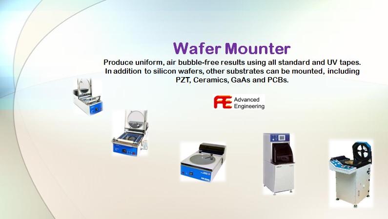
AE Advanced Engineering is a world leader in providing Dicing Environment equipment and materials to the semiconductor industry. Known for its reliable and robust products, AE develops innovative and marker-driven systems for use in the sophisticated and highly demanding microelectronics assembly market. Constantly working with its customers to help them meet ever-evolving process requirements, AE provides a wide range of dicing environment products: Wafer mounters, wafer cleaners, UV curing systems, dicing tapes and accessories Wafer Mounting: Finished wafers from a semiconductor fab are mounted on dicing tape and attached to dicing frames. Dicing: The frame-mounted wafer is placed in a dicing saw to be cut into individual dies. Cleaning: The diced wafer is placed in a wafer cleaning system to remove debris and micro-particles remaining on the wafer after the dicing process. UV Curing: Wafers that are mounted on UV curable dicing tape undergo a UV curing process to enable easy die removal for pick and place and die attach operations.

Water Treatment

X-ray Inspection


XRF Plating thickness Measurement